
Active GNSS antenna design (Part II)
Alright, here we are for the second part of the GNSS active antenna design. This time it didn’t took so long to get a new post release into the blog. I guess it’s because I haven’t been doing any online courses or anything, so more free time to play around with
…engineering!
In the last post, I described the antenna portion design. In this post I explain the LNA (Low Noise Amplifier) part, the design steps and the measurement results of the prototype.
I mentioned in the last post that for the LNA design I’ve chosen the BFP640FESD low noise BJT transistor from Infineon. Because Infineon has good documentation, has support files for simulation, it’s cheap and I had it available - problem is sometimes I trust too much on my memory, and when the PCBs for this board arrived, I realized I had not the BFP640FESD, but the BFP740F!
Oh well, I’ll explain the design steps with the BFP640FESD and use this opportunity to show what I checked and verified the impact of adapting the existing board and matching networks to the BFP740F instead of the BFP640F.
Alright, so first step is to download the S-parameter files for the transistor. Otherwise, it’s also possible to use the component models for SPICE, Keysight ADS or AWR Microwave Office - good guy Infineon having the support for all the tools. With the latter two, one can use non-linear simulations and make a more refined design. However, I’ll keep it simple and go for the design steps using the linear models (S-parameters) and design the LNA with those only. This is possible for LNAs, especially for a GNSS application, where power levels are so low that we are sure to be operating in a linear range of operation of the transistor. It would be more risky to assume something like this when designing a PA (Power Amplifier).
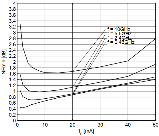
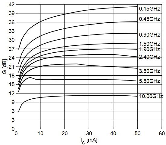
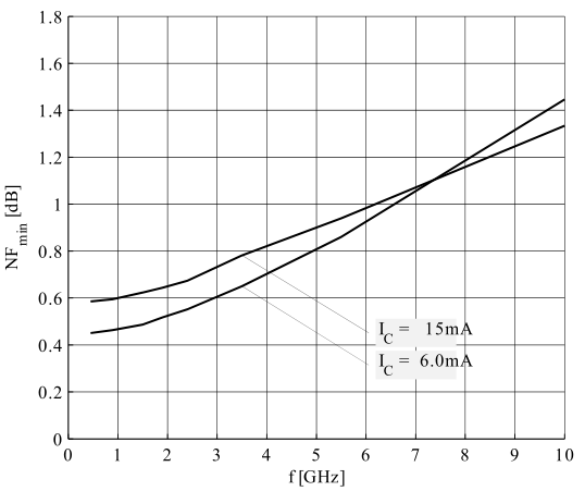
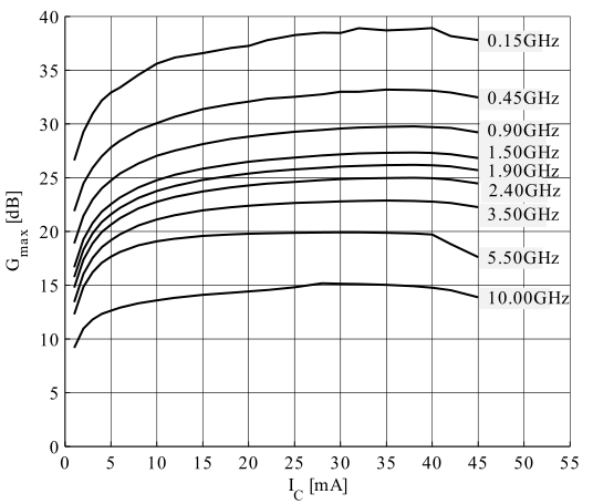
The S-parameter folder from Infineon has a bunch of files with the parameters of the transistor for different bias levels. Therefore, the first step is to choose the right bias point. For that we look into the datasheet and check the gain and noise figure plots and determine the preferable bias that will give us the operation parameters we want. The following pictures are taken from the transistor’s datasheet and show the variation of the Noise Figure and Gain with the collector current for a bias voltage of 3 V:
 |
 |
|---|---|
| Noise figure with collector current | Gain with collector current |
From the plot on the left we can see the minimal NF is attained with a low collector current, but the gain is smaller for lower currents. The compromise is to have the collector current (IC) between 20 and 30 mA. This provides a noise figure between 0.9 and 1.1 dB and a gain between 26 and 28 dB. Something in between would be preferable, but since Infineon only provides S-parameters for the 20 and 30 mA, we have to go with either one or the other and I’ll choose to go with higher gain IC = 30mA.
We fetch the S-parameters file corresponding to that bias point and from here I’ll be using QUCStudio for designing the matching networks and bias networks for the circuit. First I load the corresponding S-parameters to QUCSstudio and check the stability, noise and gain circles.
 |
 |
|---|---|
| S-parameters | Stability |
 |
 |
| S-parameters | Gain and Noise circles |
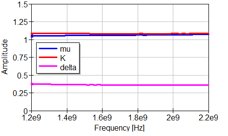
First, from the stability results we can see the transistor is unconditionally stable, that is, $\mathit{K}$ and $\mu$ > 1 and $\Delta$ < 1, this is good since we can design the matching networks for the noise/gain we want and don’t have restrictions with stability of the amplifier. To obtain the $\mathit{K}$, $\mu$ and $\Delta$ parameters we place equations in QUCS schematic as I show in the final circuit figure further down this post. The equations for the Rollet’s stability criterion ($\mathit{K}$-factor) and the Edwards-Sinsky stability criterion ($\mu$-factor), as found in Pozar’s:
\[K=\frac{1-|S_{11}|^2|-S_{22}|^2+|\Delta|^2}{2|S_{12}S_{21}|}\] \[\Delta=S_{11}S_{22}-S_{12}S_{21}\] \[\mu=\frac{1-|S_{11}|^2|}{|S_{22}-S_{11}^*\Delta|+|S_{12}S_{21}|}\]You can look into the book to know how you come to these criteria, but the principle is that if the Rollet’s stability criteria or the Edwards-Sinsky criteria are met, meaning the $\mathit{K}$ and $\mu$ are above 1, the transistor is unconditionally stable. When this does not happen, then the input and output matching networks need to be carefully designed in order to avoid getting an oscillator instead of a transistor.
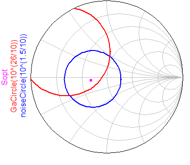
Next, we look into the Gain and Noise circles, these are generated for a NF (Noise Figure) < 1.5 and a Gain > 26 dB. There’s a zone where both these circles intersect each other. If we design our input network to match any impedance in this zone, and then design the output matching network for the complex match, we get a noise figure below 1.5 and a gain above 26 dB. For reference, I also plotted there the ‘Sopt’ which is the optimal impedance for minimum noise, which is why it is right in the center of the Noise circle. Luckily, this spot falls right in the intersection between our noise and gain circles, and besides, it is a real impedance (no imaginary part), which means a simple $\lambda$/4 line can be used to match it. These pieces seem the be falling into place quite nicely…
To get the noise and gain circles in QUCStudio, run a S-parameter simulation for a single frequency, in this case I did for 1.575 GHz, place a smith chart into the data analysis pane and plot the ‘GaCircle(x)’ and the ‘noiseCircle(y)’, where the ‘x’ and ‘y’ parameters are the gain and noise you want in linear form!
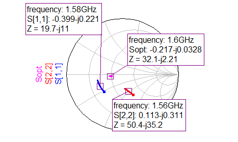
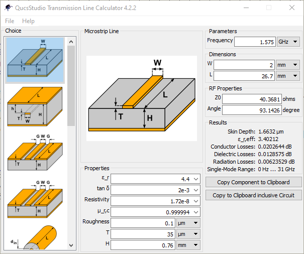
We use the line calculator embedded into QUCS to calculate that line characteristics for the input match, we know it has to have an impedance of $\sqrt{50 \times 32} = 40 \Omega$:
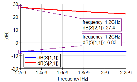
After adding this line section to the circuit input and simulating, we get the following results for the S-parameters:
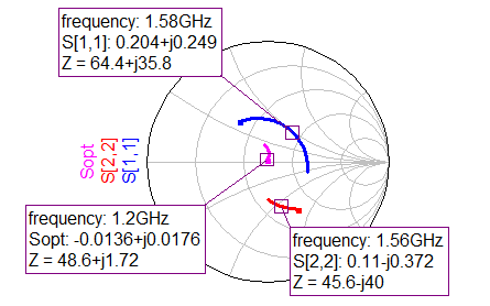
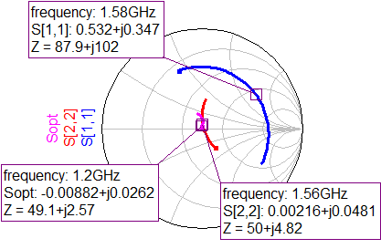
From here, we just need to do matching of the output impedance to the complex conjugate in order to get maximum power transfer, therefore, to match the impedance of 45.6-j40. This impedance is really close to 50 Ohm, hence we’ll just add a series inductor to bring it upwards in the direction of the circle center. I could do some calculations to determine the correct value of inductor to match this impedance, but my lazy ass we’ll do it the lazy way, I just add the inductor to the circuit and click “Tune” to vary the inductor value and iteratively see in the smith chart the output match moving. Which led me to a value of 6 nH and the resulting final S-parameters:
 |
 |
|---|---|
| Final S-parameters (Cartesian) | Final S-parameters (Smith chart) |
Rending a final circuit that looks like this:
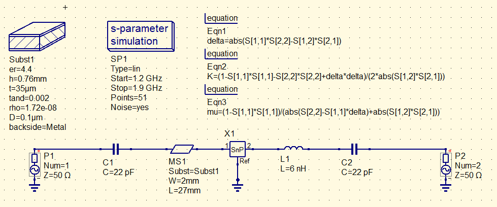
Notice the 22 pF caps at each side are DC blocks for the biasing voltages of the transistor. The high capacitance has little effect at the working frequency, but still they impose some effect, so I added those and always simulated with them so I was designing having that small effect of the DC blocks in consideration and not be surprised later on.
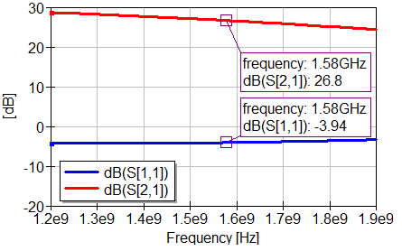
Another important thing is that the inductor in the previous circuit is ideal, which is not realistic, all components have parasitics, hence it’s important to simulate this with a more realistic model for the inductor. And using touchstone files with the measured S-parameters from the inductor supplier is a good option. So I loaded the S-parameters from a Murata inductor, and soon realized I had to use a smaller inductor value to obtain the match I was hoping for, ending up with a 5.1 nH, 0402 SMD packaged, multi-layers type inductor. Rending the final result:
A gain of above 26 dB and a NF of 1.13 in the L1 band looks good. Now the second part is to determine the circuit to make to correct bias to the transistor, that is, VCE = 3V and IC = 30 mA. For that we fill in the SPICE parameters of the transistor (can be found in Infineon application notes), and then tune the base and collector resistors to get the correct VCE voltage and collector current, as follows:
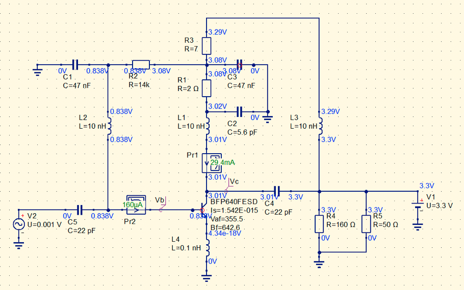
In this case, I come up to the values for R1, R2 and R3 as you see in the picture above, which for 3.3 V of input voltage, render a VCE of 3.01 V and IC of 29.4 mA, pretty close!
Well, and that’s it. We have finished our LNA!
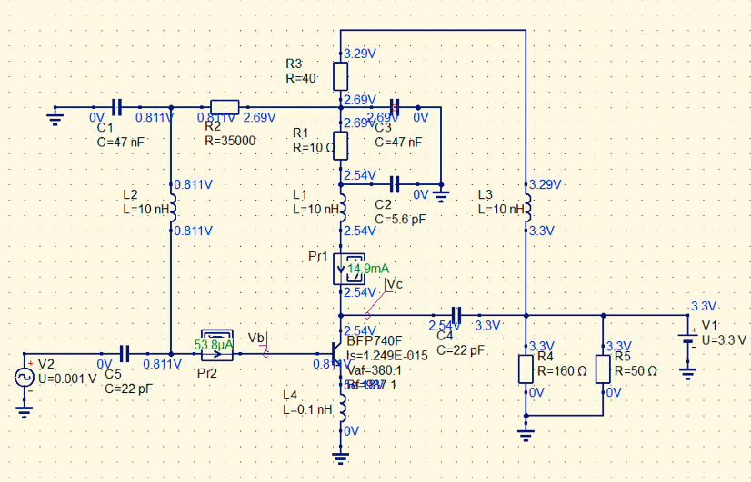
Now, remember the part where I said I screwed up and I actually had a different part in my stock? Yeah. I had BFP740F not the BFP640F… Good thing is that these transistor are not that different, even though the BFP740F is more tailored for applications around 2.4 GHz, it can still prove worthy in 1.575 GHz. Let’s check again the gain and NF plots on the datasheet, check S-parameters for the best bias point and then determine the correct bias resistors to achieve that bias point.
For the BFP740F the best spot seems to be anywhere with VCE between 2 and 3V and IC between 15 to 20 mA. I decided to go with VCE of 2.5 V and IC of 15 mA.
 |
 |
|---|---|
| Noise figure with collector current | Gain with collector current |
For that we need the following bias values:
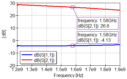
As for matching, since I couldn’t change the input matching line, I just checked what would be the final performance of the amplifier in terms of Noise Figure, and adjusted the output matching network for maximum possible gain - which I realized is actually no output matching network at all!

So, with the previously designed input matching network (a $\lambda /4$ transmission line) and no output matching at all, the final S-parameters of the LNA looked like the following:
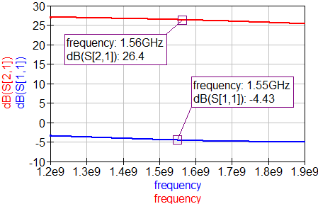
With a final NF of 1.02 and a gain of 26.4 dB, I find these results very hard to believe. So I’ll have to test the board and see how it ended up in the real thing Crossing my fingers. Next post will be about the construction of the whole thing and the measurements of the prototype. Hopefully won’t take so long to come out as this post.
Stay tuned!