UHF RFID Antennas - V - Tag dipole antennas
In the first post of this blog, I pointed out to this video about a guy discovering the wonders of UHF RFID and proposing to build his own antenna. Unfortunately for me, I discovered he knows little to nothing about antennas, and his demand has been fully about trying to replicate an already made design. That’s unfortunate for me, but doesn’t mean the video isn’t good. On the opposite, it is splendid and extremely educational. I knew all about the stuff he was talking about, and I still found it very entertaining and learned one or two other things in the process. But then I decided I could actually write a post about designing a UHF RFID tag antenna.
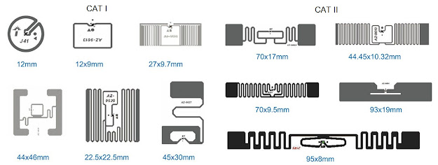
To start we need to chose a RFID chip to use, I opted for the NXP UCODE G2iM+ tag chip, because it’s easy to buy on those electronics distributors such as Mouser or Farnell and because it can be soldered. Also, instead of silver ink on paper tags, this antenna is designed on a conventional FR-4 32 mil (0.8 mm) thickness board. Also, in a real application, there would be some requirement for the dimensions of the tag, so it could fit and conform to some kind of object. In this case I don’t have any, so I defined that the tag should fit inside the following dimensions: 80 mm length by 15 mm width.
First thing to look for is the input impedance or the equivalent resistance and capacitance of the chip. In this case, NXP gives us the input impedance, $Z_c=24−j222$Ω @ 915 MHz:
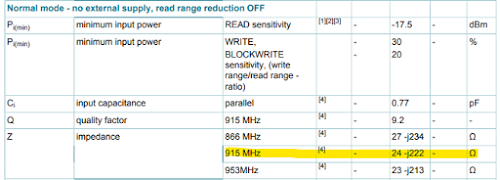
This is a complex impedance, and it is essentially capacitive - remember I said that impedances in the lower part of the Smith chart are in the capacitive zone. In order to maximize the power transfer from the antenna to the chip, the antenna impedance should be the conjugate of the chip impedance, essentially $Z_a=24+j222$Ω @ 915 MHz.
Sometimes the datasheet of RFID tags don’t give you the input impedance directly but give you the values for an equivalent linear model of the RF chip and the respective values for those components, such as the Monza R6 chip from Impinj, shown below:
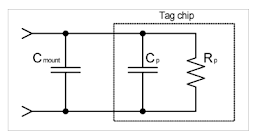
So you just have to calculate the equivalent series impedance of this circuit $Z_s=R_s+jX_s$Ω , and $R_s$ and $C_s$ can be obtained from the following:
\[R_s=\frac{R_p}{1+Q_p^2}\] \[X_s=\frac{X_p}{1+\frac{1}{Q_p^2}}\] \[Q_p=\frac{R_p}{X_p}\]And if you don’t remember, the equivalent impedance of the capacitor is given by:
\[X_p=\frac{1}{j2\pi f_0C_p}\]Using these expressions, the equivalent series impedance of the Monza R6 chip at 915 MHz is $Z_c=16.4−139.5$Ω or $Z_c=12.0−j119.6$Ω if you account for the mounting capacitance ($C_{mount}$), which you should (as mentioned on the datasheet)!
How to go about the design? Well, if you look at the description on this paper by Rao and Nikitin, RFID tag antennas are designed to be resonant at higher frequencies than the intended frequency of operation, so that at some point at lower frequencies, it matches the conjugate of the chip impedance. Something like in the following picture:
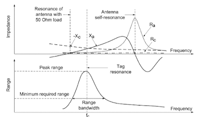
Maybe we can start to design an antenna that has it’s reactive part zero at the desired frequency, and then apply a matching network to transform it’s impedance to the chip conjugate impedance. Sounds simple enough… Let’s start with the dipole!

So I went bananas with the dipole design and decided to add some random flavoring to the tips. And now you’re asking ‘Why?’. Well, because it looks cool! There’s guys doing RFID tags with Louis Vuitton brand logos and calling it a scientific paper, so why not? Here it is:

How did I come to that design? Well, I started with the premise that to fit inside the dimensions I wanted, I had to go for a meandered dipole structure. Then I just tuned the spacing between the meanders and the section width, until I reached a reactance of 0 Ohm @ 915 Mhz. The input impedance of the antenna is shown in the following picture:
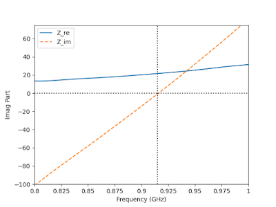
Now we just need to add an inductive ring so that it can sport a reactance of around 220 Ohm. That’s quite considerable, so the inductive ring should have some considerable size. I’ve added the following (spoiler alert: it was not big enough):

So we get…
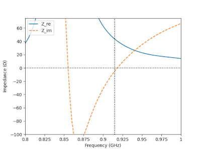
What the hell?! Let’s look at the big picture:
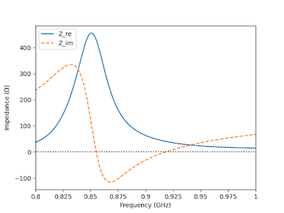
Well, that certainly was unexpected… Or was it?

Well, that loop also increased the size of the dipole… Considerably! But it did what was intended, it certainly raised the antenna reactance. That’s something that can be worked with! We simply need to pick on the length of the dipole to readjust the resonance to a upper frequency (as demonstrated on Rao’s paper mentioned previously), while adjusting the ring perimeter and width to get the right impedance value. Let’s take a closer look at the previous result, but wider bandwidth:
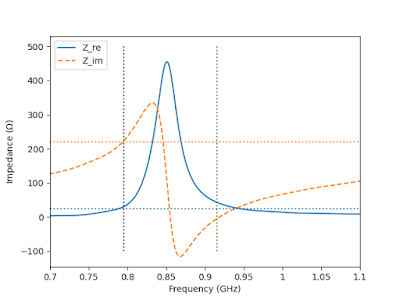
Actually, we nearly achieved impedance values closed to the intended ones, but at the wrong frequency, at 795 MHz in this case (marked with the black dotted line). There, let’s just wiggle around with the dipole length to get the resonance higher (reducing the dipole arms overall length) so we can move that to the vertical green dotted line. Then we’ll make fine adjustments to the ring in order to get the correct impedance, but for that, we need to understand the influence of the ring perimeter and the location of the ring with respect to the feed point. So if we change the length (Lring) of the inductive feed ring, we of course get a higher reactance, and slightly lower resonant frequency. But if we change the width (Wring), therefore, changing the feed distance to the ring, then we get a smaller change in reactance (to a comparable increase in perimeter increase) and a slight increase on the resonating frequency. This is shown in the following pictures:
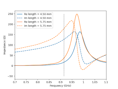
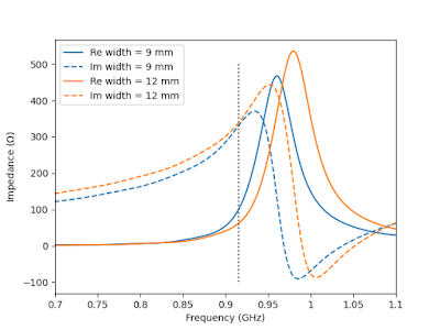
So, with these relationships in mind, and also with the length of the dipole, in this case by making small adjustments to the length between the last arm section and the ‘M’ termination (Ltune), we can make a few sweeps until we reach the spot! 😎
And we end up with something like the following:

I’ll post the .dxf of the antenna on my GitHub page (coming soon, look on the left side) so you can import it to a PCB. Just remember that dimensions are set in millimeters and that the bottom layer of the PCB should have no copper at all! The impedance response with frequency is shown in the following picture. And if we normalize the input impedance to the conjugate of the chip impedance, we can view the frequency response in our beloved S-parameter equivalence.
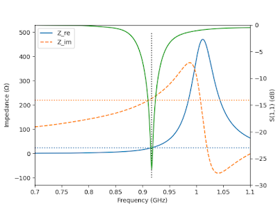
And, as well said in Rao’s paper I mentioned above in this post, the most important parameters for a tag, is the reading range you can achieve with it. Thankfully, they have a nice expression to help us calculate the theoretical range we could achieve with this tag, given by the following:
\[r=\frac{\lambda}{4\pi}\sqrt{\frac{P_tG_tG_r\tau}{P_{th}}}\]where:
- $P_t$ is the transmitted power by the reader antenna
- $G_t$ is the gain of the reader antenna
- $G_r$ is the gain of the tag antenna
- $\tau$ which represents the matching between the chip impedance and antenna impedance, and is given by: $\tau=\frac{4R_cR_a}{|Z_c+Z_a|^2}$
- $P_{th}$ which is the minimum power threshold to activate the tag
Being $Z_c=R_c+jX_c$ the chip impedance and $Z_a=R_a+jX_a$ the antenna impedance.
If this resembles the Radar equation to you, well, that’s because it is the Radar equation! With a slight adaptation to make it fit the backscatter narrative with the $\tau$ and the $P_{th}$ parameters. Also notice that this expression does not account for de-polarization losses. But it is safe to assume it especially if we’re using a circularly polarized antenna at the reader. We just need to remember to use the circularly polarized gain of the antenna in the Gt term, instead of the maximum gain.
To calculate the reading range we have nearly all the parameters, except for the gain of the tag antenna (for the gain of the reader antenna, we’ll be using the values from the dual-feed microstrip patch antenna from my previous post). So let’s take a look at the radiation characteristics of the tag antenna. The following picture shows the farfield radiation pattern as well as the $E_{\theta}/E_{\phi}$ relation, that will indicate the polarization direction of the radiation. The maximum antenna gain of the tag is rather low, at around 1 dBi. But that’s fairly usual. Smaller tags than this can have even smaller gains. It’s not so uncommon to find UHF RFID tag antennas with gains around -3 dBi.
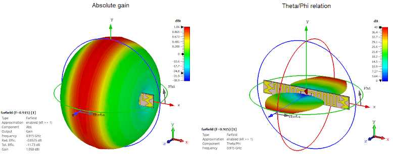
From the above plot on the right, the polarization is linear and horizontal (along X axis). One can also look at the surface current variation:

But this time the surface current distribution could be misleading, because the highest current density is focused around the inductive ring and there the current flows up and down. But, if you look closely, when the current is pointing down on the left, its pointing up on the right side of the ring. This inversed current flow will nullify each other, so the current flow is either pointing towards the right or the left at any given time. Hence, we have a linear and horizontal (along X axis direction) polarization.
For the purpose of estimating the reading range of this tag, I’ve considered the output power of the reader to be 1 W (30 dBm), the limit by FCC regulation, the $P_{th}$ of the tag as given in the datasheet of -17.5 dBm, which with the gains mentioned and with the impedances simulated for the tag antenna, we reach the following result:
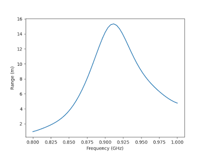
That’s nearly 15 meters of reading range. Pretty impressive, but well, this is all theoretical. In practice the range is probably much smaller, but I believe it can probably achieve ranges in the order of 10 meters.
Well, that’s it for today folks! This was a rather long post. I’ll try to manufacture this one but I have to find some way to test it, since I no longer have my UHF RFID reader. I’ll eventually post results if I find a way to test it.
Stay tuned!
