
UHF RFID Antennas - VII - Quadrifilar antenna (Part II)
To continue on the topic of the printed quadrifilar antennas, as promised, this post will be about the feeding network. Last post I’ve shown the antenna part and a quick explanation as to what the feeding network should look like, this time I’m going to cover the power distribution network that makes it all work. More specifically, I’ll explore an alternative that allows the antenna construction to be more compact and with better performance.
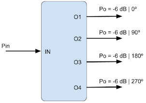
So the idea is to create a system which has one single input port and four output ports, where all the outputs have the same power and 90º sequential phase difference between them, as explained in the last post.
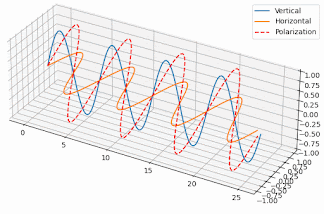
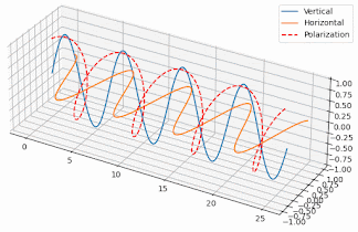
But how exactly does that work and why the antenna becomes circularly polarized, when the single element of the antenna has linear polarization? Well, if you generate two orthogonal electric field components with a 90º phase difference between them, then the resulting field in the direction of radiation varies circularly. To the left or to the right depending on which component comes first. Here’s two poor animations I’ve put together in Python to illustrate the effect (I made an effort alright?):
 |
 |
|---|---|
| Electric field components with 0º phase | Electric field components with 90º phase |
So, since we have elements generating linear polarization but one orthogonal to the other, if they’re fed in phase, they’ll generate a linear, but slant polarization, like the animation on the left. But, if they’re fed with a 90º phase difference we get a circular polarization, like the one shown on the right.
If you’d like to see something with better looks and a more detailed explanation, then look no further and check out this video about polarization of electromagnetic waves.
And now you’re wondering, “Wait, but if you only need to excite two fields with 90º phase between them, then why do you have an antenna with 4 elements, what are the other two elements for?”

Now seriously, the other two elements are there to balance the main-lobe direction. You see, the only way to make it with only two elements, is if the two elements are physically co-located, so that their phase centers are in the same spot. SPOILER ALERT: This is possible, but that’s another pots. Since in the example of the quadrifilar antenna each element is apart from another, their phase-centers are separated, this will cause the radiation pattern to tilt towards the opposite side of the fed elements.
 |
 |
|---|---|
| Only two elements fed | All four elements fed. |
The continuous phase progression is easy to understand given that the other elements are in opposition of phase. The element in the bottom is generating an electric field with the exact same polarization component, but in opposition of phase, the same happens to the element of the left side in relation to the element on the right. If these were to be fed in phase, the field components would cancel between them, and you end up with…

With that out of the way, let’s get back to the point of this post, which is about the feeding network as shown in the first figure. Now, as my grandma used to say, “there’s many ways to tie a tie”, so there’s many ways to produce said feeding network. The most obvious and straightforward method is as I’ve shown in my previous post:
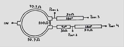
It’s a Wilkinson power divider, followed by delay lines. The main issue with this implementation, is that a microstrip line with quarter-wavelength length (90 degrees of electrical length) in FR-4 substrate at 900 MHz, is 46.1 mm long, and for that implementation you have one branch with 180º, that’s 92.2 mm and the other with 270º, that’s a whooping 138.3 mm length. Of course you can make curves and meander it around, but that’s still a lot of track to cover. And when you think that these lines have a huge loss given FR-4 being a very poor substrate material for RF tracks, you really start to look for better alternatives.
One alternative is as shown in Qiang Liu’s paper, which is actually a combination of two structures, first an out-of-phase (180º) power splitter, described in J. X. Chen’s paper, plus two miniaturized arbitrary phase difference couplers, as described in Yongle Wu’s paper. As in the following picture:
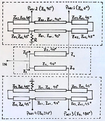
NOTE: I could have done this schemes in a computer, but I’m lazy-artistic and I enjoyed doing them on hand.
The middle section represents the out-of-phase power splitter and the top and bottom sections are the arbitrary phase difference couplers, in this case, tuned for 90º phase difference between ports.
Let’s break it down…

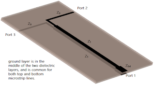
The out-of-phase power splitter is actually a pretty simple and clever structure. It’s made with two microstrip lines on top of each other, with a common ground plane in the middle, and the signal is fed into one of the lines with respect to the other, so they’re naturally out-of-phase (180º). In order to accomplish the 50 Ω impedance at the output ports, an impedance transition of 25 to 50 Ω is necessary, which is achieved with a quarter-wavelength section of line with $Z_1=Z_0/2–\sqrt(2)=35.35$Ω . Here’s an illustration of that section (ground plane is hidden so bottom layer is visible).
The coupler is a little more complex, nevertheless, the principle for design is not complicated. There’s essentially two different sections, one at the middle with the highest impedances, and the left and right sections, being equal, with lower impedances. They’re composed of coupled microstrip line sections, with a given length and even/odd impedance characteristic, determined based on the intended phase delay between each of the ports. These impedances can be calculated from the following expressions:
\[Z_{e1}=2k\sqrt{1−C^2}\sin\phi/[(k+1)C]\] \[Z_{e2}=\sqrt{Z_{e1}^2/(1+Z_{e1}Z_{o1})}\] \[Z_{o1}=Z_{e1}/k\] \[Z_{o2}=Z_{e2}/k\]where $C$ is the coupling coefficient, 3-dB in this case, and $\phi$ is the phase difference between ports, 90º in this case. The $k$ factor is a value between 1 and 2, that balances the bandwidth of operation of the coupler, with its potential size and design constraints. In Qiang Liu’s paper they’ve set $k$ to 1.2, which is a good compromise between size, bandwidth and the feasible separation between tracks for fabrication, wielding the following parameter values for the couplers lines, $Z_{e1}=54.5 \Omega$, $Z_{o1}=45.5 \Omega$, $Z_{e2}=38.5\Omega$ and $Z_{o2}=32.0 \Omega$.
So now you just need to design said couplers and you’re rightfully asking, “how to design such coupled lines with those even and odd mode impedances?”. Well, there are some closed form equations to determine the physical parameters of the lines based on the impedance parameters, and the easiest and fastest way is to use an online calculator, like this one, instead doing all those calculations by hand.Here’s an example of one of the sections with $Z_{e1}$ and $Z_{o1}$ impedances:
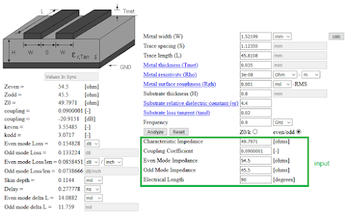
As you can see, with those values for even/odd impedance, the width and separation spaces for the coupled microstrip lines are very close to the dimensions used by Qiang Liu in his paper. Still, this is just to obtain an approximate result, these are then further optimized in simulation, and given the wide bandwidth of operation, working with just slide deviations is ok.
All of this put together results in the following:
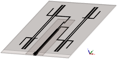
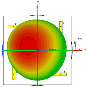
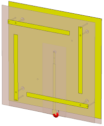
The ground plane is transparent in this picture so all the layers are visible. Nevertheless, between the top and bottom PCB’s, there’s a common ground for both microstrip lines, it’s border can be seen in the bottom section of the picture, at the input section, there’s no ground in between the two feed pads. Then, when combined with the four PIFA antennas from before, placed at a distance from 11.2 mm from the ground plane of the couplers board, result in the following structure, wielding the results shown:
 |
 |
|---|---|
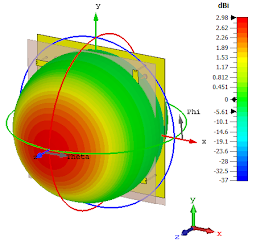
| Complete quadrifilar structure perspective view | Radiation pattern (Gain) at 900 MHz |
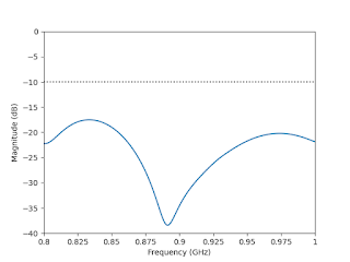 |
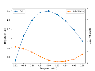 |
| Reflection coefficient | Gain and axial-ratio with frequency |
The impedance bandwidth as well as the circular polarization bandwidth are quite wide. But the trade-off is the gain, especially when implementing such a distribution network on a very lossy substrate, reducing the radiation efficiency to values in the order of 70%, the maximum RHCP gain is 3.0 dBic.
I wanted to show another method to have a sequential phase difference 4-port distribution network, but this post is getting rather long, so I’m going to leave that to a further opportunity. As usual, I’ll upload the design files for this antenna on my GitHub.
Stay tuned!