
Vertical Interconnect Accesses - Do you even RF? (Part II)
A while ago I promised to look into the effects of using VIAs (Vertical Interconnect Access) on RF tracks to change layers on PCBs. Unlike the 90º degree bends on PCB tracks, in this case there’s essentially two postures about the matter. Either people are completely clueless of the potential risk of placing a via on a RF track and do it recklessly. Or they’re somehow a little aware of the risks, therefore completely demonize such practice, going at extreme lengths such as increasing the track sizes immensely (making it even worst), just so to avoid the use of the via.
A long time ago I found an awesome primer about vias for high-speed and RF tracks from Keysight, you can find it here. However, it focuses mainly on multi-layer board in excess of 8 layers. Therefore, although the concepts are the same and the material is absolutely valuable no matter your scenario, it lacks the actual results you’d get in a 2 or 4 layer board.
I’ve been cooking this post for a while, but due to several reasons (laziness), it has taken me much longer than usual to finish it up. And then, in the latest weeks there’s been releases on Youtube, of videos concerning this very specific topic, about ground vias and current return paths. So, instead of going through a lengthy post and a lot of explanations, I’m just going to leave here two links for two videos from Mr. Robert Feranec’s youtube channel explaining why this stuff matters and showing some neat simulations on the phenomena.
Video 2 - Current return paths
Now, this stuff is no secret, you can read the High-Speed Digital Design: A Handbook of Black Magic by Howard W. Johnson and Martin Graham and you’d learn most of this stuff. The issue is, most electronics engineers don’t actually read this book unless they work with Signal Integrity topics, but believe me if I say everyone can benefit from getting to know about it. And not only those poor EMC engineers, that have to dwell into the deepness of electronic hell, to fight the evil forces of the electromagnetic and restore the balance to the force(s)… quite literally.

(me, fightning the nasty harmonics. Or the way I picture it in my head…)
Well, that would be a pretty lame post if I’d just leave it at that. So I’m going to try to show the limits of the application of vias on RF tracks, especially in 2- and 4-layer FR-4 PCBs, which are used most frequently, especially (but not exclusively) in the hobbyist world.
Let’s start with the 2-layer PCB. Now you could be legitimately asking why would someone need to know this, who’d be the fool to design RF circuits on 2-layer FR-4 PCBs…

That is legit, but you’d be surprised how much this is common ground nowadays, surf a little bit about, on such as the Hackaday, to see the amount of projects with wireless communications on it using 2-layer PCBs. The simulation structure is microstrip line, tuned for 50 Ω , split in the middle with a via from top to bottom layer. The main issue with this practice, in this particular scenario, is that the reference ground for the track on the top is on the bottom layer, but when you shift the signal to the bottom layer, the ground reference for the new track is now on the top layer. The inductance increase by the increased return path is such that obliterates the impedance response of the track, becomes a radiation source and simply messes the signal for any RF frequency. Again, if you’re working at 10 MHz you probably don’t need to worry about this, but if you’re using a Bluetooth module at 2.45 GHz, you better pay attention!
Here’s the simulation models for 2-layers and 4-layers examples:
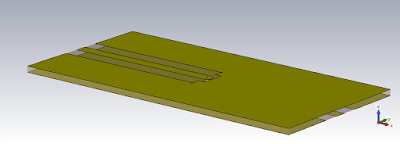
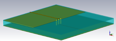
For the 2-layer example I’ve modeled the dielectric as FR-4, while for the 4-layer board I’ve based the PCB on the OSH Park 4-layer stackup.
In scenario I, there’s no vias connecting the plane, but since the boundaries of the simulation model, at widths edge, are modeled as perfect electrical conductors, both planes will touch this and will have the same potential. On scenario II, I added some vias close to the transition via. I also simulated with boards of 1.6 and 0.8 mm thicknesses to see the possible improvement a smaller via could provide, making up scenario III and IV. This leads to the following results:
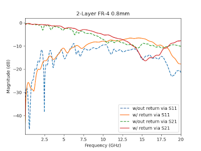
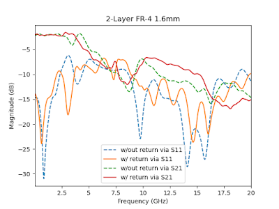
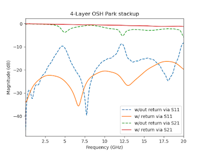
If we break down these results, one thing is clear, don’t even try to change layers of an RF track if you’re designing on a 2 layer FR-4 PCB of 1.6 mm of thickness, no return vias will save your ass. I mean, the vias certainly improve a little bit, allow you to go a little beyond 2 GHz, but the performance is just trash anyway. Now, if you’re smarter, you’d use a 0.8 mm board, well then the proper use of return vias will allow you to go up to 5 GHz without much trouble. But, fail to provide a decent return path and you’ll be facing problems already at 2.5 GHz. Now if you look at the results for the 4-layer PCB, it gives you two things: 1) OSH Park 4-layer PCB stackup, with their permittivity controlled ISOLA substrate, is wicked good for RF designs; 2) the return vias have a considerable effect in this scenario. As you can see from the results above, if you have a correct return path you can do transitions on the RF tracks with vias and go way beyond 10 GHz without breaking a sweat.

But, if you fail to provide said decent return path, you may get away with a passable, but not good performance. Remember that these simulation models are quite small, they’re just a section of the PCB with the track within and even in the no via case the return path is a short distance away since the edges of the PCB are shorted at the boundary and have the exact same potential all along the sides. In a real application this is not the case! Both planes will retain the same potential as long as there’s vias connecting them both, besides, the tracks will probably be longer. Hence, take this results as optimistic bacause in a real PCB it’s gonna be worst!
One thing I haven’t explored in depth in here, is the radiation effects. But if you check those videos from Mr. Feranec he explains the effects of slots on the return path and what are the outcomes of such foul practices.
That’s all for today folks, I hope my next post will not take as long to come out.
Stay tuned!